1Learning Outcomes
Identify properties of a memory circuit.
Describe the behavior of a positive edge-triggered d-type flip-flop.
Identify setup time, hold time, and clk-to-q delay in a FF timing diagram.
Explain the importance of setup time and hold time for sampling an input.
🎥 Lecture Video
As we’ve seen in a previous section, combinational logic circuits provide all the necessary functions needed to execute instructions, including all the arithmetic and logic operations, incrementing the program counter value, determining when to branch,calculating the new PC target values, etc, but they have no memory of their previous inputs or outputs. The memory circuit[1] is an example of another type of circuit used to make processors that does remember its inputs. This memory circuit is used to implement the general purpose register, as shown in Figure 1.
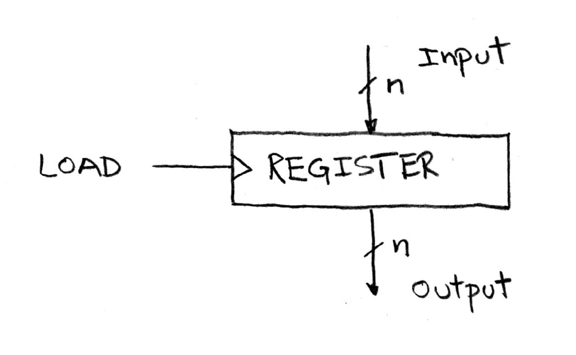
Figure 1:Diagram of a register implemented through a memory circuit.
2The General Register: A Memory Circuit
Under the control of a special input, called LOAD, the register captures the value of the input signal and holds onto it indefinitely, or until another value is loaded. The value stored by the register appears at the output of the register (a very short time after it gets loaded). If the processor loads a value in a register at one point in time, it can come back later and read that same value back. Even if different values appear at the input to the register in the interim, the output value of the register will not change unless instructed to do so by signaling with the LOAD input. So, as long as the processor has control over the signaling of the LOAD input, it has total control over what gets saved and when.
Often the system clock signal CLK (see The Clock), is used as the LOAD signal on a register, as shown in Figure 2. This configuration means that, for this register, a new value is loaded on each clock cycle. This is a valuable configuration we will explore in a [future section].
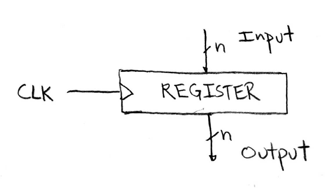
Figure 2:Diagram of a clocked register implemented through a memory circuit.
3What’s inside a register?
As shown in Figure 3, an n-bit wide register is nothing other than n instances of a simpler circuit[2].
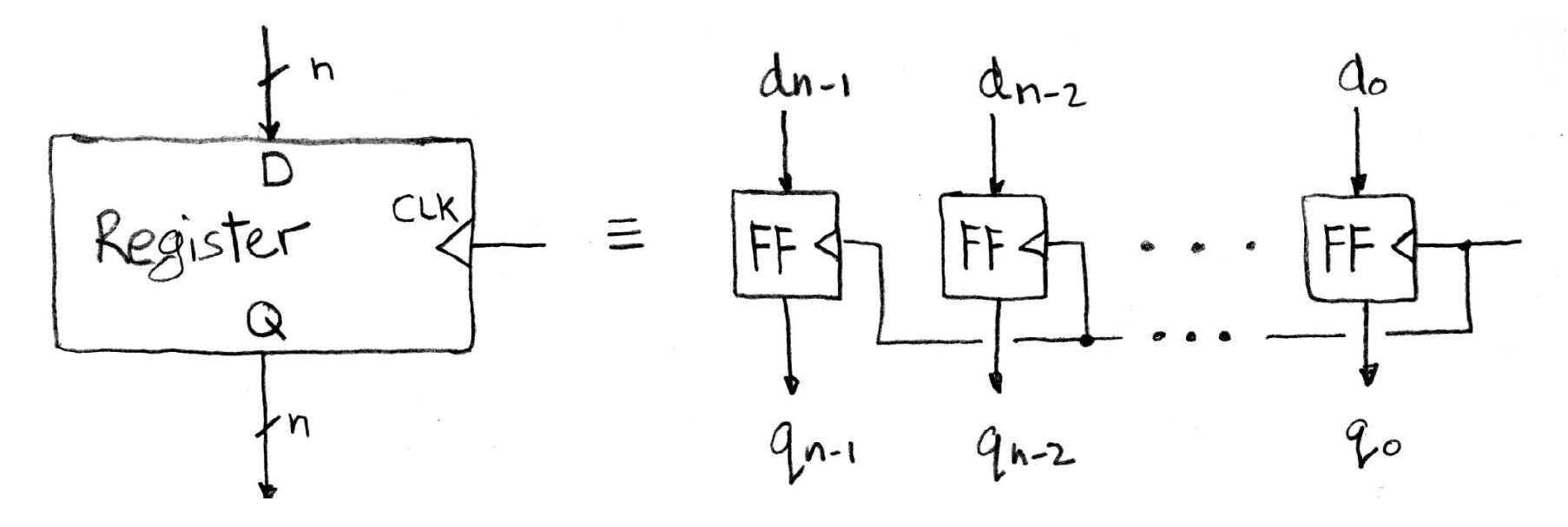
Figure 3:Diagram of a register built from n instances of simpler circuits called flip-flops.
3.1Flip-Flops
We call these simple circuits flip-flops (FF), which are 1-bit wide registers named from the fact that when in operation, it flips (and flops) between holding a 0 or a 1. The CLK (or LOAD) signal is sent to the CLK (or LOAD) input of all n FFs. Each FF is responsible for storing one bit of the n-bit data stored by the register. By register convention, the input is labeled D and the output is labeled Q. In the case of a single bit, the input is labeled d and the output is labeled q.
3.2Edge-Triggered D-Type Flip Flop
The most common type of FF is called the edge-triggered d-type flip flop. Internally, each FF comprises around 10 transistors. The operation of the FF is illustrated as a waveform diagram in Figure 4. The figure shows the operation of a positive edge-triggered d-type flip-flop, one of two types of edge-triggered d-type flip-flops. Negative edge-triggered d-type flip-flops is the other type, but for CS 61C, we will focus on positive edge flip-flops.
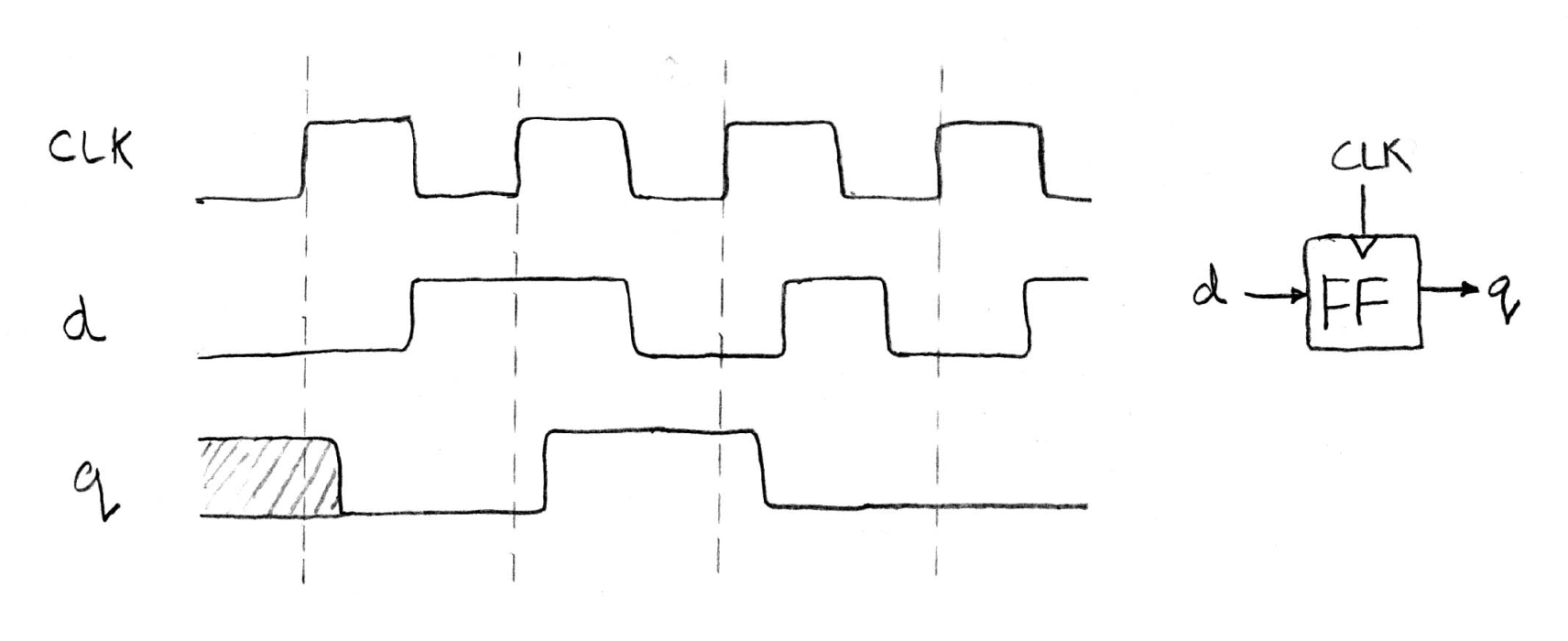
Figure 4:Waveform diagram of the operation of an edge-triggered d-type FF.
3.3Positive Edge-Triggered D-Type Flip-Flops
For positive edge-triggered d-type FFs, on each positive (rising) clock edge, the d input is sampled and transferred to the q output. At all other times, the d input is ignored.
Click to see an example simulator wavefrom diagram!
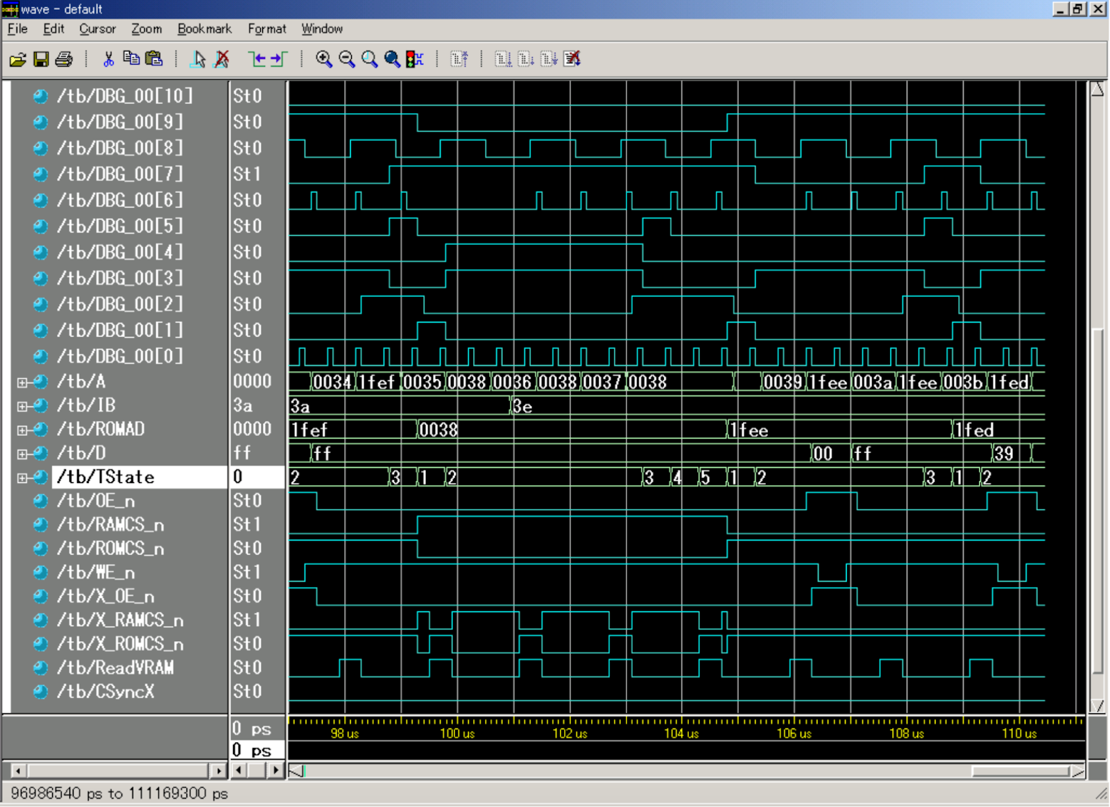
Figure 5:Simulator waveform diagram for a positive d-type FF.
3.4FF Timing Diagram
A detailed FF timing diagram for a positive edge-triggered d-type FF is shown in Figure 6. Like combinational logic circuits, FFs cannot change their outputs instantaneously. Additionally, time is needed to transfer inputs internally. Therefore, the d input must be stable for a short amount of time before the rising clock edge (called the setup time) and remain stable for a short amount of time after the edge (called the hold time). Together, the setup and hold times create a time window when the d input cannot change. If it changes in this window, the FF will not reliably capture the new input. Note that, once the FF captures the new input in response to the rising clock edge, it also takes a small amount of time to transfer the new value to the output (called the clk-to-q delay)[3].
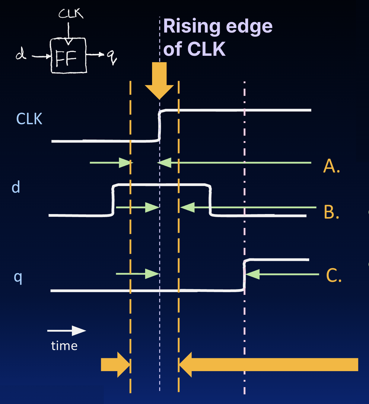
Figure 6:Timing diagram of a positive edge-triggered d-type FF.
Looking at Figure 6 above:
Aillustrates the setup time.Billustrates the hold time.Cillustrates the clk-to-q delay.The vertically dashed yellow lines illustrate the time window during which the input
dmust be stable (from the start of the setup time until the end of the hold time).
These notes are adapted from Professor John Wawrzynek’s notes: SDS Handout.
These notes are adapted from Professor John Wawrzynek’s notes: State Handout.
There is no particular relation between hold time and clk-to-q delay, because the former describes the input and the latter describes the output. However, in practice hold time is less than clk-to-q delay.